- 您现在的位置:买卖IC网 > Sheet目录310 > AP8800AWT-7 (Diodes Inc)IC LED DRIVER TSOT23-5
AP8800A
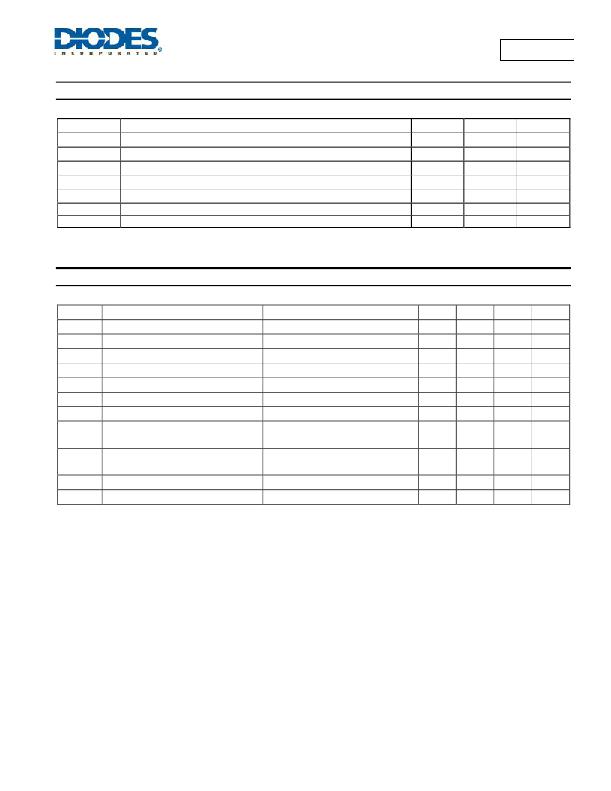
Recommended Operating Conditions (@T A = +25°C, unless otherwise specified.)
Symbol
V IN
V CTRLDC
V CTRLL
I SW
D PWM
f SW
T A
Parameter
Operating Input Voltage Relative to GND
Voltage Range for 24% to 200% DC Dimming Relative to GND
Voltage Low for PWM Dimming Relative to GND
Continuous Average Switch Current (Note 4)
Duty Cycle Range Applied to CTRL (f < 500Hz)
Switching Frequency
Ambient Temperature Range
Min
8.0
0.3
0.01
-40
Max
28
2.5
0.2
370
1
600
105
Unit
V
V
V
mA
kHz
°C
Note:
4. Dependent on junction and ambient temperature.
Electrical Characteristics (@T A = +25°C, V IN = 12V, unless otherwise specified.)
Symbol
Parameter
Conditions
Min
Typ
Max
Unit
I Q
I SD
V THD
V REF
I SET
R DS(ON)
I SW-LKG
f SW
t SS
t PD
θ JA
Quiescent Current
Shutdown Current
Internal Threshold Voltage
Internal Reference Voltage
SET Pin Input Current
On Resistance of MOSFET
Switch Leakage Current
Switching Frequency with L = 100μH
Soft-Start Time
Internal Comparator Propagation Delay
Thermal Resistance Junction-to-Ambient
V CTRL = 1.25V, f SW = 250kHz
V CTRL = 0V
V SET = V IN -0.1
ADJ pin floating L = 100H
I OUT = 350mA @ 1 LED (V LED = 3.4V)
Time taken for output current to reach 90%
of final value after V CTRL = 0.3V
TSOT25 (Note 5)
95
300
20
100
1.25
1.3
1.5
250
500
55
200
650
30
105
2.2
5
μA
μA
mV
V
μA
?
μA
kHz
μs
ns
° C/W
Note:
5. Test condition for TSOT25: Device mounted on FR-4 PCB (25mm x 25mm 1oz copper, minimum recommended pad layout on
top layer and thermal vias to bottom layer ground plane. For better thermal performance, larger copper pad for heat-sink is needed.
AP8800A
Document number: DS35100 Rev. 3 - 2
3 of 13
www.diodes.com
August 2012
? Diodes Incorporated
发布紧急采购,3分钟左右您将得到回复。
相关PDF资料
AP8800FNG-7
IC LED DRIVER HIGH BRIGHT 10DFN
AP8801M8G-13
IC LED DRIVER HIGH BRIGHT 8MSOP
AP8802HSP-13
IC LED DRIVER HIGH BRIGHT 8SOIC
AP8802SPG-13
IC LED DRIVER HIGH BRIGHT 8SOIC
AP8803WTG-7
IC LED DRIVER CONN CURR TSOT23-5
APEK4402KLP-01-T-DK
BOARD EVAL FOR A4402
APP-001-15AMP
PLUG AUTO PWR BLACK W/LED 15AMP
APP-001-20AMP
AUTO PLUG 12VOLT WITH 20AMP FUSE
相关代理商/技术参数
AP8800EV1
功能描述:AP8800 1, Non-Isolated Output LED Driver Evaluation Board 制造商:diodes incorporated 系列:- 零件状态:有效 电流 - 输出/通道:300mA 输出和类型:1,非隔离 电压 - 输出:- 特性:可调光 电压 - 输入:8 V ~ 28 V 所含物品:板 使用的 IC/零件:AP8800 标准包装:1
AP8800EV2
功能描述:AP8800 1, Non-Isolated Output LED Driver Evaluation Board 制造商:diodes incorporated 系列:- 零件状态:有效 电流 - 输出/通道:300mA 输出和类型:1,非隔离 电压 - 输出:- 特性:可调光 电压 - 输入:8 V ~ 28 V 所含物品:板 使用的 IC/零件:AP8800 标准包装:1
AP8800FNG-7
功能描述:LED照明驱动器 28V, 350mA LED DC/DC Converter RoHS:否 制造商:STMicroelectronics 输入电压:11.5 V to 23 V 工作频率: 最大电源电流:1.7 mA 输出电流: 最大工作温度: 安装风格:SMD/SMT 封装 / 箱体:SO-16N
AP8800M8G-13
功能描述:LED照明驱动器 28V, 350mA LED DC/DC Converter RoHS:否 制造商:STMicroelectronics 输入电压:11.5 V to 23 V 工作频率: 最大电源电流:1.7 mA 输出电流: 最大工作温度: 安装风格:SMD/SMT 封装 / 箱体:SO-16N
AP8800SG-13
功能描述:LED照明驱动器 28V, 350mA LED DC/DC Converter RoHS:否 制造商:STMicroelectronics 输入电压:11.5 V to 23 V 工作频率: 最大电源电流:1.7 mA 输出电流: 最大工作温度: 安装风格:SMD/SMT 封装 / 箱体:SO-16N
AP8800SG-13-CUT TAPE
制造商:DIODES 功能描述:AP8800 Series 350 mA 28 V 600 kHz SMT LED Step-Down Converter - SOIC-8L
AP8801
制造商:DIODES 制造商全称:Diodes Incorporated 功能描述:500mA LED Step-Down Converter
AP8801_0912
制造商:DIODES 制造商全称:Diodes Incorporated 功能描述:500mA LED Step-down Converter
